Embedded Protocol I2C
I²C (Inter-Integrated Circuit) is a bi-directional two wires and serial data transmission communication protocol developed by Philips (Now NXP Semiconductor) in 1982. I2C is a Half-duplex communication protocol – (I2c can’t send and receive same time in the bus-data line). Multi-master can communicate with multi-salve. (Note: Communication is restricted between two masters; however, a single master can communicate with either a single slave or multiple slaves.) I2C is a Level Triggering. A device that sends data onto the bus is defined as a transmitter, and a device receiving data is defined as a receiver.
The bus must be controlled by a master device, responsible for generating the Start and Stop conditions. In contrast, certain devices such as LCDs, EEPROMs, and RTCs function as slaves. It’s important to note that both master and slave devices can operate as either transmitters or receivers. However, the master device plays a pivotal role in determining which mode is activated.
Applications & Uses
- I2C Applications : System Management Bus (SMBus), Power Management Bus (PMBus), Intelligent Platform , Management Interface (IPMI), Display Data Channel (DDC), Advanced Telecom Computing Architecture (ATCA)
- I2C Uses : I2C can be used to control a wide range of devices: analogue-to-digital and digital-to-analog converters (ADCs and DACs), LCD and OLED displays, keyboards, LED and motor drivers, memory chips and cards (EEPROM, RAM, FERAM, Flash), pressure and temperature sensors and other peripheral devices.
- I2C GPIO Extender – Microchip’s MCP23008(8channel), Microchip’s MCP23017(16channel), Texas Instruments pcf8574(8chennel).
- I2C RTC (DS1337).
Feature
- 1000 different IC’s manufactured are available 50 more companies.
- There’s an allowance for multiple clock-masters on the same bus
| Feature | Description |
|---|---|
| Master-Slave Architecture | One device acts as the master, controlling communication, while others are slaves responding to commands. |
| Bi-Directional Communication | With the SDA and SCL lines facilitating the transmission and reception of data on the same lines, the I2C protocol ensures efficient bidirectional communication. |
| Multi-Master Support | Multiple master devices can exist on the same bus with proper coordination. |
| Addressing | Each device has a unique address, and the master specifies the target device before communication. |
| Clock Synchronization | The master generates the clock signal, synchronizing the timing of data transfer. |
| Start and Stop Conditions | Communication begins with a start condition and ends with a stop condition, indicating the data transfer’s start and end. |
| Acknowledgment | After each byte transfer, the receiving device sends an acknowledgment signal to confirm successful reception. |
Revisions
| Year -Version | Description |
|---|---|
| 1982 | 100 KHz I²C Simple Internal Bus (Philips Chips) |
| 1992 – Version 1 | 400 KHz fast Mode (Fm) 10 Bit addressing mode 1008Nodes First Standardized Version 400 Kbit/s |
| 1998-Version 2 | 3.4 MHz High Speed mode (Hs) Power saving requirement for electric voltage and current 3.4 Mbit/s |
| 2000 – Version 2.1 | Minor clean-up of version 2 |
| 2007 – Version 3 | 1 MHz Fast mode plus (Fm+) Device ID Mechanisms 1 Mbit/s |
| 2012 – Version 4 | 5 MHz Ultra-fast mode (UFm) New USDA and USCL lines using push pull logic without pull-up resistors Added assigned manufacturer ID table |
| 2012 – Version 5 | Corrected mistakes |
| 2014 – Version 6 | Corrected graph, This is most recent standard |
Operating Speed Mode
| Type | Mode | Speed | Applications |
|---|---|---|---|
| Bidirectional Bus | Low speed mode | 10 Kbit/s | |
| Standard mode (Sm) | 100 Kbit/s | ||
| Fast mode (Fm) | 400 Kbit/s | Embedded Systems & PCs usual Speed | |
| Fast mode plus (Fm+) | 1 Mbit/s | ||
| High Speed mode (Hs-mode) | 3.4 Mbit/s | ||
| Unidirectional Bus | Ultra-Fast mode (UFm) | 5 Mbit/s |
Addressing methods
I2C Addressing 7Bit
- In the 7-bit addressing mode, comprising 128 address lines, the system allows a maximum of 112 slave nodes to be connected to the masters.
I2C Addressing 10bit
- In the 10-bit addressing mode, which provides a vast address space with 1024 address lines, a maximum of 1008 slave nodes can be connected to the masters.
- Two address words are used for device addressing instead of one.
- The first address word MSBs are conventionally coded as “11110” so any device on the bus is aware the master sends a 10 bits device address

I²C Address Allocation Table
The group number represents the hexadecimal equivalent of the four most significant bits of the slave address (A6-A3).
- Note : X = Don’t care, A = Programmable address bit, P = Page selection bit
Address Allocation Table Group 01 to 05
| GROUP(1) | TYPE NUMBER | DESCRIPTION | ||
|---|---|---|---|---|
| Group 0 (0000 | ||||
| 0 | 0 | 0 | – | General call address |
| X | X | X | – | Reserved addresses |
| Group 1 (0001) | ||||
| 1 | A1 | A0 | SAA2530 | ADR/DMX digital receiver |
| 1 | A1 | A0 | TDA8045 | QAM-64 demodulator |
| Group 2 (0010) | ||||
| 0 | 0 | A0 | SAA4700/T | VPS dataline processor |
| 0 | 0 | A0 | SAA5233 | Dual standard PDC decoder |
| 0 | 0 | 1 | SAA5243 | Computer controlled teletext circuit |
| 0 | 0 | 1 | SAA5244 | Integrated VIP and teletext |
| 0 | 0 | 1 | SAA5245 | 525-line teletext decoder/controller |
| 0 | 0 | 1 | SAA5246A | Integrated VIP and teletext |
| 0 | 0 | 1 | SAA5249 | VIP and teletext controller |
| 0 | A1 | A0 | CCR921 | RDS/RBDS decoder |
| 0 | A1 | A0 | SAF1135 | Dataline 16 decoder for VPS (call array) |
| 1 | 0 | 0 | SAA5252 | Line 21 decoder |
| 1 | 1 | A0 | SAB9075H | PIP controller for NTSC |
| Group 3 (0011) | ||||
| 0 | 0 | A0 | SAA7370 | CD-decoder plus digital servo processor |
| 0 | A1 | A0 | PCD5096 | Universal codec |
| 0 | 1 | A0 | SAA2510 | Video-CD MPEG-audio/video decoder |
| 0 | 1 | 1 | PDIUSB11 | Universal serial bus |
| 1 | 0 | 1 | SAA2502 | MPEG audio source decoder |
| 1 | 1 | A0 | SAA1770 | D2MAC decoder for satellite and cable TV |
| Group 4 (0100) | ||||
| 0 | 0 | 0 | SAA6750 | MPEG2 encoder for Desk Top Video (=SAA7137) |
| 0 | 0 | 0 | TDA9177 | YUV transient improvement processor |
| 0 | 0 | 0 | TDA9178 | YUV transient improvement processor |
| 0 | 0 | A0 | PCA1070 | Programmable speech transmission IC |
| 0 | A1 | A0 | PCF8575 | Remote 16-bit I/O expander |
| 0 | A1 | A0 | PCF8575C | Remote 16-bit I/O expander |
| 0 | A1 | A0 | SAA1300 | Tuner switch circuit |
| A2 | A1 | A0 | TDA8444 | Octuple 6-bit DAC |
| A2 | A1 | A0 | PCF8574 | 8-bit remote I/O port (I2C-bus to parallel converter) |
| 1 | 0 | A0 | PCD3311C | DTMF/modem/musical tone generator |
| 1 | 0 | A0 | PCD3312C | DTMF/modem/musical tone generator |
| 1 | 1 | 1 | PCD5002 | Pager decoder |
Address Allocation Table Group 06 & 07 (Cont..)
| GROUP(1) | TYPE NUMBER | DESCRIPTION | ||
|---|---|---|---|---|
| Group 6 (0110) | ||||
| 0 | 0 | 0 | SAA5301 | MOJI processor for Japan/China |
| 0 | 1 | 1 | PCE84C467/8 | 8-bit CMOS auto-sync monitor controller |
| 0 | 1 | 1 | PCE84C882 | 8-bit microcontroller for monitor applications |
| 0 | 1 | 1 | PCE84C886 | 8-bit microcontroller for monitor applications |
| Group 7 (0111) | ||||
| 0 | 0 | A0 | SAA7140B | High performance video scaler |
| 0 | 0 | A0 | PCF8533 | Universal LCD driver for low multiplex rates |
| 0 | 0 | A0 | PCF8576 | 16-segment LCD driver 1:1 – 1:4 Mux rates |
| 0 | 0 | A0 | PCF8576C | 16-segment LCD driver 1:1 – 1:4 Mux rates |
| 0 | A1 | A0 | SAA1064 | 4-digit LED driver |
| A2 | A1 | A0 | PCF8574A | 8-bit remote I/O port (I2C-bus to parallel converter) |
| 0 | 1 | 0 | PCF8577C | 32/64-segment LCD display driver |
| 0 | 1 | A0 | PCF2103 | LCD controller/driver |
| 0 | 1 | A0 | PCF2104 | LCD controller/driver |
| 0 | 1 | A0 | PCF2105 | LCD controller/driver |
| 0 | 1 | A0 | PCF2113 | LCD controller/driver |
| 0 | 1 | A0 | PCF2119 | LCD controller/driver |
| 0 | 1 | A0 | SAA2116 | LCD controller/driver |
| 1 | 0 | A0 | PCF8531 | 34 X 128 pixel matrix driver |
| 1 | 0 | A0 | PCF8548 | 65 X 102 pixels matrix LCD driver |
| 1 | 0 | A0 | PCF8549 | 65 X 102 pixels matrix LCD driver |
| 1 | 0 | A0 | PCF8578/9 | Row/column LCD dot matrix driver/display |
| 1 | 0 | A0 | PCF8568 | LCD row driver for dot matrix displays |
| 1 | 0 | A0 | PCF8569 | LCD column driver for dot matrix displays |
| 1 | A1 | A0 | PCF8535 | 65 X 133 pixel matrix LCD driver |
| 1 | 1 | A0 | OM4085 | Universal LCD driver for low multiplex rates |
| 1 | 1 | A0 | PCF8566 | 96-segment LCD driver 1:1 – 1:4 Mux rates |
Address Allocation Table Group 08 (Cont..)
| GROUP(1) | TYPE NUMBER | DESCRIPTION | ||
|---|---|---|---|---|
| Group 8 (1000) | ||||
| 0 | 0 | 0 | TEA6300 | Sound fader control and preamplifier/source selector |
| 0 | 0 | 0 | TEA6320/1/2/3 | Sound fader control circuit |
| 0 | 0 | 0 | TEA6330 | Tone/volume controller |
| 0 | 0 | A0 | NE5751 | Audio processor for RF communication |
| 0 | 0 | A0 | TDA8421 | Audio processor |
| 0 | 0 | A0 | TDA9860 | Hi-fi audio processor |
| 0 | 0 | 1 | TDA8424/5/6 | Audio processor |
| 0 | 1 | 0 | TDA8415 | TV/VCR stereo/dual sound processor |
| 0 | 1 | 0 | TDA8417 | TV/VCR stereo/dual sound processor |
| 0 | 1 | 0 | TDA9840 | TV stereo/dual sound processor |
| 0 | 1 | A0 | TDA8480T | RGB gamma-correction processor |
| 1 | 0 | 0 | TDA4670/1/2 | Picture signal improvement (PSI) circuit |
| 1 | 0 | 0 | TDA4680/5/7/8 | Video processor |
| 1 | 0 | 0 | TDA4780 | Video control with gamma control |
| 1 | 0 | 0 | TDA4885 | 150 MHz video controller |
| 1 | 0 | 0 | TDA8442 | Interface for colour decoder |
| 1 | 0 | 1 | TDA8366 | Multistandard one-chip video processor |
| 1 | 0 | 1 | TDA8373 | NTSC one-chip video processor |
| 1 | 0 | 1 | TDA8374 | Multistandard one-chip video processor |
| 1 | 0 | 1 | TDA8375/A | Multistandard one-chip video processor |
| 1 | 0 | 1 | TDA8376/A | Multistandard one-chip video processor |
| 1 | 0 | 1 | TDA9161A | Bus-controlled decoder/sync. processor |
| 1 | A1 | 1 | SAA7151B | 8-bit digital multistandard TV decoder |
| 1 | A1 | 1 | SAA7191B | Digital multistandard TV decoder |
| 1 | A1 | 1 | SAA9056 | Digital SCAM colour decoder |
| 1 | A1 | 1 | TDA9141/3/4 | Alignment-free multistandard decoder |
| 1 | A1 | 1 | TDA9160 | Multistandard decoder/sync. processor |
| 1 | A1 | 1 | TDA9162 | Multistandard decoder/sync. processor |
| 1 | 1 | 0 | TDA4853/4 | Autosync deflection processor |
| 1 | 1 | 0 | TDA9150B | Deflection processor |
| 1 | 1 | 0 | TDA9151B | Programmable deflection processor |
| 1 | 1 | A0 | TEA6360 | 5-band equalizer |
| 1 | 1 | A0 | TDA8433 | TV deflection processor |
Address Allocation Table Group 09 (Cont..)
| GROUP(1) | TYPE NUMBER | DESCRIPTION | ||
|---|---|---|---|---|
| Group 9 (1001) | ||||
| A2 | A1 | A0 | PCF8591 | 4-channel, 8-bit Mux ADC and one DAC |
| A2 | A1 | A0 | TDA8440 | Video/audio switch |
| A2 | A1 | A0 | TDA8540 | 4 X 4 video switch matrix |
| 1 | A1 | A0 | TDA8752 | Triple fast ADC for LCD |
| 1 | 1 | A0 | SAA7110A | Digital multistandard decoder |
Address Allocation Table Group A to C (Cont..)
| GROUP(1) | TYPE NUMBER | DESCRIPTION | ||
|---|---|---|---|---|
| Group A (1010) | ||||
| 0 | 0 | A0 | SAA7199B | Digital multistandard encoder |
| 0 | 1 | 0 | TDA8416 | TV/VCR stereo/dual sound processor |
| 0 | 1 | A0 | TDA9850 | BTSC stereo/SAP decoder |
| 0 | 1 | A0 | TDA9855 | BTSC stereo/SAP decoder |
| 0 | 1 | 1 | TDA9852 | BTSC stereo/SAP decoder |
| 1 | 0 | 0 | TDA9610 | Audio FM processor for VHS |
| 1 | 0 | 0 | TDA9614H | Audio processor for VHS |
| 1 | A1 | 0 | SAA7186 | Digital video scaler |
| 1 | 0 | 1 | PCA8516 | Stand-alone OSD IC |
| 1 | 1 | 1 | SAA7165 | Video enhancement D/A processor |
| 1 | 1 | 1 | SAA9065 | Video enhancement and D/A processor |
| Group B (1011) | ||||
| 0 | 0 | A0 | SAA7199B | Digital multistandard encoder |
| 0 | 1 | 0 | TDA8416 | TV/VCR stereo/dual sound processor |
| 0 | 1 | A0 | TDA9850 | BTSC stereo/SAP decoder |
| 0 | 1 | A0 | TDA9855 | BTSC stereo/SAP decoder |
| 0 | 1 | 1 | TDA9852 | BTSC stereo/SAP decoder |
| 1 | 0 | 0 | TDA9610 | Audio FM processor for VHS |
| 1 | 0 | 0 | TDA9614H | Audio processor for VHS |
| 1 | A1 | 0 | SAA7186 | Digital video scaler |
| 1 | 0 | 1 | PCA8516 | Stand-alone OSD IC |
| 1 | 1 | 1 | SAA7165 | Video enhancement D/A processor |
| 1 | 1 | 1 | SAA9065 | Video enhancement and D/A processor |
| Group C (1100) | ||||
| 0 | 0 | 1 | TEA6100 | FM/IF for computer-controlled radio |
| 0 | 1 | 0 | TEA6821/2 | Car radio AM |
| 0 | 1 | 0 | TEA6824T | Car radio IF IC |
| 0 | A1 | A0 | TSA5511/2/4 | 1.3 GHz PLL frequency synthesizer for TV |
| 0 | A1 | A0 | TSA5522/3M | 1.4 GHz PLL frequency synthesizer for TV |
| 0 | 1 | A0 | TDA8735 | 150 MHz PLL frequency synthesizer |
| 0 | 1 | A0 | TSA6057 | Radio tuning PLL frequency synthesizer |
| 0 | 1 | A0 | TSA6060 | Radio tuning PLL frequency synthesizer |
| 0 | 1 | A0 | UMA1014 | Frequency synthesizer for mobile telephones |
| 1 | 0 | 0 | TDA8722 | Negative video modulator with FM sound |
Address Allocation Table Group D to F (Cont..)
| GROUP(1) | TYPE NUMBER | DESCRIPTION | ||
|---|---|---|---|---|
| Group D (1101) | ||||
| 0 | 0 | A0 | TDA8043 | QPSK demodulator and decoder |
| 0 | 0 | A0 | TDA9170 | YUV processor with picture improvement |
| 0 | A1 | A0 | PCF8573 | Clock/calendar |
| A2 | A1 | A0 | TDA8443A | YUV/RGB matrix switch |
| 0 | 1 | A0 | TDA8745 | Satellite sound decoder |
| 1 | 0 | 0 | TDA1551Q | 2 ´ 22 W BTL audio power amplifier |
| 1 | A1 | A0 | TDA4845 | Vector processor for TV-pictures tubes |
| 1 | A1 | A0 | UMA1000T | Data processor for mobile telephones |
| 1 | 1 | A0 | PCD4440 | Voice scrambler/descrambler for mobile telephones |
| Group E (1110) | ||||
| 0 | 0 | 0 | PCD3316 | Caller-ID on Call Waiting (CIDCW) receiver |
| 0 | 0 | 0 | TDA9177 | 2nd address for LTI (1st is ’40’) |
| 0 | 0 | 0 | TDA9178 | 2nd address for LTI (1st is ’40’) |
| 0 | 0 | A0 | SAA7192 | Digital colour space-converter |
| Group F (1111) | ||||
| X | X | X | – | Reserved addresses |
| Group 0 to F (0000 to 1111) | ||||
| X | X | X | PCF8584 | I2C-bus controller |
I2C Basic Design

SDA (Serial Data Line)
This pin serves a bidirectional purpose, transferring addresses and data both into and out of the device. It is an open-drain terminal.
Hence, the SDA bus necessitates a pull-up resistor to VCC (typically 10k Ω for 100 kHz, 2 kΩ for 400 kHz). During normal data transfer, SDA can change only during SCL low, reserving alterations during SCL high specifically for indicating the Start and Stop conditions.
SCL (Serial Clock Line)
The input clock synchronizes the data transfer to and from the device. The master generates all clock pulses, including the acknowledged clock pulse.
- Master device (Master node)
- Node that generates the clock and initiates communication with slave
- Slave device (Slave node)
- Functioning as a node that receives the clock and responds exclusively when addressed by the master, this device plays a pivotal role in the I2C communication protocol.
- The address space and the total bus capacitance of 400 pF collectively limit the maximum number of nodes.
- Note : Basically SDA and SCL Open drain (So need Pulled up resistor)
I2C Message Protocols
I²C defines basic types of messages, each of which begins with a START and ends with a STOP:
- Single message where a master writes data to a slave;
- Single message where a master reads data from a slave;
- Combined messages, where a master issues at least two reads and/or writes to one or more slaves.
Master & Salve function
| Device | Function Role |
|---|---|
| Master device |
|
| Slave device |
|
| Transmitter/Receiver |
|
I2C Physical Layer

- Device count limit: max capacitance 400pF
I2C Pull-up resistor
Centrally suggest used Pull-up resistor for i2c communication scl and sda line is 2Kohm for 100Kbps and 10Kohm for 400Kbps. Refer this : http://www.ti.com/lit/an/slva689/slva689.pdf
I2C Minimum pull-up resistor value
- Furthermore, determining the minimum resistance is straightforward and relies on factors such as the bus voltage (Vbus), the maximum voltage considered as a logic-low (VOL), and the maximum current that the pins can sink when at or below VOL (IOL).
- Formula : Rp(min) = (Vbus – VOL) / IOL
I2C Minimum pull-up resistor value
- The maximum pull-up resistance is based on the needed rise-time of the clock (dependent on the I2C clock frequency), and the total capacitance on the bus. The I2C specification (http://cache.nxp.com/documents/user_manual/UM10204.pdf) lists the maximum total bus capacitance with a pull-up resistor to be 200 pF (it can be up to 400 pF if the pull-up is a current source, section 5.1). This specification also describes the rise-time of SDA/SCL to be a maximum of 300 ns in “Fast-mode” – 400 kHz.
- Formula : Rp(min) = rt / ( 0.8473 * Cb )
- Here, rt represents the maximum allowed rise-time of the bus, and Cb denotes the total bus capacitance.
I2C Pull-up resistor Example
- Rp(Max) = tr/(0.8473*Cb) = (3000*10^-9)/(0.8473* (200*10^-12)) = 1.77kohm
- Rp(Min) = (Vcc-Vol)/Iol = (3.3-0.4)/3*10^-3) = 966.667ohm
I2C Data Frame
It operates in a byte-oriented transmission mode.
I2C Bus Characteristics

- Initiation of data transfer is permissible only when the bus is not busy (free).
- During data transfer, the data line must remain stable whenever the clock line is high. Interpretation of changes in the data line while the clock line is high as a Start or Stop condition takes place.
- An Acknowledge bit must follow each byte.
I2C Bus Busy :
- During the transition from the Start (S) to the Before (P) state, the protocol unfolds a series of critical events.
I2C Bus Free :
- Before the Start (S) and after the Stop (P) conditions, the I2C protocol encompasses crucial states that dictate the initiation and conclusion of data transfer.
- While both data and clock lines remain high, the system awaits the initiation of the next phase in the communication process.
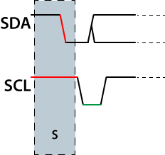
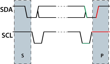
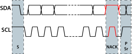
I2C Start (S) Condition
- A high-to-low transition of the SDA line while the clock (SCL) is high determines a Start condition. All commands must be preceded by a Start condition.
I2C Stop (P) Condition
- The occurrence of a low-to-high transition on the SDA line, while the clock (SCL) is high, serves as the determinant for a Stop condition. All operations must end with a Stop condition.
I2C Repeated Start (Sr) Condition

I2C Data Valid condition
- Each data transfer is initiated with a Start condition and terminated with a Stop condition. The number of the data bytes transferred between the Start and Stop conditions is determined by the master device.
I2C data transfer condition
- Data is transferred with the Most Significant Bit (MSB) first. An Acknowledge bit must follow each byte.
I2C read/write conditions
- The last bit of the control byte holds significance as it defines the operation to be performed. Specifically, when set to ‘1,’ a read operation is selected, whereas when set to ‘0,’ a write operation is chosen.
I2c Acknowledgement (ACK) Condition
- When a device acknowledges, it must pull down the SDA line precisely during the Acknowledge clock pulse, ensuring the SDA line remains stable-low throughout the high period of the Acknowledge-related clock pulse.
- The master generates all clock pulses, including the acknowledged clock pulse.

I2C Not Acknowledgement (NACK) Condition
I2C Clock Synchronization

I2C Clock Stretching

If a slave is pulling the clock down, it’s called “clock-stretching” and is a signal to the master to pause until the slave is ready.
The Below diagram is raspberry bi i2c clock stretching

I2C Arbitration
- Bus arbitration will be handled by Masters (Not slave)
- What will happens if the two masters are write different data to same slave-1 in I2C?
- What will happens if the two masters are write same data to same slave-1 in I2c?
- How to know the data of master-1 or master-2 writes same data in slave-1?(conditions : if two masters are write same data to same slave-1, in I2c)
- What will happens if the two masters are read data from same slave-1 in I2c?
I2C Single master with multi-slave connection diagram

i2C Multi-Master with Multi-Slave connection diagram
- At the same time can’t able to communicate with one more master.

I2C LM75 Temperature Data format Example
Example 1 :
When employing the LM75 temperature sensor in its simplest mode, the master initiates the process by sending the address along with a read bit. Subsequently, it reads two bytes back. Noteworthy is that since the master transmitted the address, the slave promptly acknowledges, indicating its readiness for further communication. Then the slave sends a byte, which the master acknowledges with an ACK. Then the slave sends the second byte, to which the master responds with a NACK and a stop signal to say it’s done.
Master: Start Signal
Master: Address + Read Bit
Slave:  ACK
Slave:  First byte of data
Master: ACK
Slave:  Second / last byte of data
Master: NACK
Master: Stop Signal
Example 2 : Concluding the protocol, there are also instances of multi-part communications. For instance, if the master intends to transmit a byte to the slave and subsequently read multiple bytes, it follows a sequence. Initially, the master sends the address with a write signal and then retransmits the address with a read signal. To signify the change in mode, the master employs the “repeated start” signal, essentially a regular start signal when there has been no preceding stop. To illustrate, consider the LM75 example, where the master first signals its intention to read the high-temperature setting and subsequently reads the two bytes back.
Master: Start Signal
Master: Address + Write Bit
Slave:  ACK
Master: Set the high-temperature register for reading
Slave:  ACK
Master: (Re-) Start Signal
Master: Address + Read Bit
Slave:  ACK
Slave:  First byte of data
Master: ACK
Slave:  Second / last byte of data
Master: NACK
Master: Stop Signal
I2C Advantages & Disadvantage
Advantage
- Only uses two wires
- Supports multiple masters and multiple slaves
- The ACK/NACK bit affirms the successful transfer of each frame.
- Hardware is less complicated than with UARTs
- Well-known and widely used protocol
Disadvantages
- Slower data transfer rate than SPI
- The data frame size is limited to 8 bits
- More complicated hardware needed to implement than the SPI
Tools and Analyzer
- Aardvark I²C/SPI Host Adapter
- Bitscope Logic
- Bus pirate logic Analyzer
- Corelis I²C Bus Analyzer
- MCC-I²C Tools
Simulator of I2C
I2C Interface Example
- ESP8266 NodeMCU Module I2C : https://aruneworld.com/embedded/esp8266/esp8266-nodemcu/esp8266-nodemcu-module-i2c/
- ESP32 NodeMCU Module I2C : https://aruneworld.com/embedded/esp32/esp32-nodemcu/esp32-nodemcu-module-i2c/
- PIC Micro-Controller interface with I2C : https://electrosome.com/i2c-pic-microcontroller-mplab-xc8/
Refer Websites
- Wikipedia_I²C
- Everything about I²C
- Official I²C specification (free), NXP
- List of assigned NXP / Philips I²C addresses (free), NXP
- 7-bit, 8-bit, and 10-bit I²C Slave Addressing
- PDF – I²C-bus specification n and user manual By NXP
- https://www.I²C-bus.org
- https://www.byteparadigm.com/applications/introduction-to-i2c-and-spi-protocols/
- https://en.m.wikipedia.org/wiki/Bit_banging
- http://codinglab.blogspot.com/2008/10/i2c-on-avr-using-bit-banging.html
- http://dlnware.com/dll/I2C-Bus-Interface-CC-API
- https://hackaday.com/2016/07/19/what-could-go-wrong-i2c-edition/
- How communicate two I²C masters? : https://www.I²C-bus.org/multimaster/
- I2C YouTube Videos :
- https://youtu.be/RPHP4fAisz8
- I2c Protocol Analyzer Tool Video : https://www.youtube.com/watch?v=Ggvw8K12FuE
You must be logged in to post a comment.