A Printed Circuit Board (PCB) is a fundamental component in modern electronics manufacturing. It serves as a platform for mechanically supporting and electrically connecting electronic components. These consist of a non-conductive substrate material, typically fiberglass, with conductive pathways etched or printed onto the surface to form circuits.

PCBs play a crucial role in virtually all electronic devices, from simple consumer electronics like smartphones and computers to complex industrial machinery and aerospace systems. They provide a compact and reliable means of interconnecting electronic components while minimizing space requirements and manufacturing costs.
In real-world applications, the PCB alone is just one part of the process PCBA takes it further by integrating the components onto the board through soldering and placement techniques. This assembled form is what powers nearly every modern electronic device you interact with.
These will come in various types and configurations, including single-sided, double-sided, and multi-layered designs, depending on the complexity of the circuit and the application requirements. Advanced manufacturing techniques, such as surface-mount technology (SMT) and through-hole technology (THT), allow for precise component placement and soldering on Boards, enabling high-density and high-performance electronic assemblies.
In summary, These are the backbone of electronic systems, providing the necessary foundation for the integration and operation of electronic components, making them essential in modern technology.
Get Start with PCB Design
If your going to design then you need to know the following details for before start design
Requires :
- Case size
- Board size
- Hole size
- Components size(Selected Componets)
- Design(Circuit)
- Now Start design using tool
- Set Board Border
- set place of Holes
- Set Place of all components
- Set Place the all components name
- Clearance should more than 12mil for best
- track also 12mil for best
File Format
CAD Format
dwg – AutoCAD Drawing.
- Autodesk created .dwg in 1982 with the very first launch of AutoCAD software. DWG files contain all the information that a user enters in a CAD drawing. This data can include:
- Designs
- Geometric data
- Maps and photos
Image Source
dxf – AutoCAD Drawing Interchange Format.
- Add soon
Auto Desk
Auto CAD Android App

- Android app from play-store : Download
Eagle PCB
EAGLE design software is an affordable, easy to use yet powerful tool for designing printed circuit boards. This award winning software offers user friendly powerful and affordable solutions for design, including Schematic Capture, Board Layout and Autoroute
- Image 1 Source

- Image 2 Source
Eagle PCB – File Format
- xxxx.lbr – Library file
- xxxx.sch – Schematic file
- xxxx.brd – board file
- xxxxx.ulp – User Language program
Eagle PCB – Libraries
Image Source

- Libraries – All of the parts that you place on your designs are stored in libraries. Each part will contain a device, symbol, and package.
- Devices. Within every library, you’ll have one or multiple devices. These devices include both a schematic symbol and a package in one accessible location.
- Symbols. Within every device, you’ll have a symbol, which provides a visual representation of a part for use on a schematic.
- Packages. Within every device, you’ll also have a package, which is the physical representation of a part for use in a PCB layout.
- Pads. The pads are the red rectangles on this part and are numbered according to your datasheet. When placed on a PCB, each of these pads will be connected to a trace and provide electrical connectivity for a part.
- Package Dimension. The package dimension is the rectangular gray outline that you see connecting all of the pads. This outline represents the actual physical dimensions of your part can help during your PCB layout prhttps://www.autodesk.com/products/eagle/blog/wp-content/uploads/2017/03/package-numbered.pngocess to see if you’re placing components too close together.
- Silkscreen Outline. The silkscreen outline is the rectangular yellow lines lying over the gray package dimension lines. While this piece is optional, it helps to provide a visual indicator for your manufacturer when they are assembling parts on your bare board.
- Name and Value. These text elements are placeholders and will come in handy during your PCB layout stage. As the text suggests, Name will be used to identify the unique name of your part when you place it on your PCB layout, and Value can be utilized for things like labeling the resistance of a resistor, capacitance of a capacitor, etc…
Image Source

Note : 1. Pad, 2.package Dimension, 3.Silkscreen Outline, 4. Name and Value
Others Eagle Libraries.
- ArunEworld Eagle Libraries
- ELement14 Eagle CAD library – Contains all major electronics parts
- Honeywell.lbr by Robertstarr – Contains some pressure sensors and other foot prints
- SparkFun Eagle Libraries – SparkFun’s Public Eagle PCB Footprints using Eagle 6.0+ or greater.
Eagle PCB – Create a new libraries
Follow Steps
- Open a Eagle application and you can see the control panel.
- Select File » New » Libraries (You can get new library panel)
- Before creating any new parts, you need to save your library by selecting File » Save (or Cmd + S on Mac and Ctrl + S on Windows)
- Now that your library is saved, you just need to activate it. Go back to your Control Panel, right-click your new library, and select Use. You’ll know if your library is ready to go if it has a green dot next to it in your Control Panel.
Image Source

Note : if you are a library creator you should know the each detail of device like foot print and everything. refer datasheet.
AutoCAD Drawing Viewer

- Download : https://autocad-drawing-viewer.en.softonic.com/
- Pros
- Allows viewing of AutoCAD files without AutoCAD
- Allows basic editing of AutoCAD files
- Allows finding and replacing of block attribute values
- Cons
- Editing power is very basic
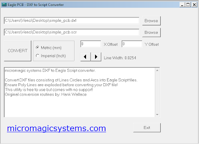
Eagle PCB DXF to SCR Converter (251Kb zip Win32 App)
DXF2SCR Converter – a FREE utility to convert DXF files consisting of lines circles and arcs into Eagle PCB script files which can then be imported into your PCB layout. Supports metric and imperial, X and Y drawing offset and line width. DXF polylines need to be exploded before importing. Output is placed on the Dimension layer.
Drawing a PCB by exact dimensions using EAGLE PCB isn’t quite the easy thing. An easier approach would be to draw it in AutoCAD and then import. Importing is quite easy. This is how it goes. This is my simple pcb 😀
Now what you need is to save the drawing to DXF format by going to Save As and chose AutoCAD 2004 DXF form the Files of type drop down menu. Name your file and save it.
Follow The Steps
Image Source

- Load the file and hit convert. You need to provide destination for both input and output file.
Image Source

- Now you go to EAGLE PCB and select File -> Script. Find the SCR file and open it. Now you should see the exact same PCB form the AutoCAD drawing.
- However you will need to place holes and drills. Those you see now are drawn on the Dimensions layer AND WILL NOT FORM ANY ACTUAL DRILLS. Here is a trick that helps me dealing with this.
- It is wise to put some sort of a mark for the center of the holes when drawing the PCB in AutoCAD. A small cross would do just fine. After importing the drawing to EAGLE those crosses will be used as a markers to show the exact place of the holes and drills. This is how I do it:
- After the import you need to zoom in to the center. Turn your grid on (I use dots) and carefully align the center of the hole and the marker. Take note that after the import the grid is set to Finest(which is 1 mil) You might need to use the Change command to make the lines 0 mils in width. It’s easier to see the grid this way. Now use the move command to get the hole or drill. The holes are usually placed on the schematic so they have names like H1, H2 .. etc. To grab the hole just type its name in the command line.
- It is a tricky job but with some practice you will get used to it 🙂 When you are finished aligning the holes you can delete the markers. Now you change your grid back to normal.
Reference : AutoCAD to EAGLE PCB Drawing Import
Import DXF into Eagle
- Reference : https://learn.sparkfun.com/tutorials/importing-custom-images-into-eagle/method-2-import-dxf
Cloud Converter
Home Made PCB
What you can do
- You can make single/double sided PCBs at home (Make Your Own Printed Circuit Boards in Minutes!)
- Easiest method to make a homemade PCB for prototyping
- Easiest way to learn making PCB
- Fast method to make simple layout PCBs at home
- Step-by-step guide to building your own PCB boards complete with photos and video illustrations
Required
Make PCB using followings
- Paper
- Yellow TTP (Toner Transfer Paper).
- A4 Tracing Paper (Desmat A4 tracing Paper). or 5 Star film UV rays (Hydrogen Peroxide)
- Thermal Heat Transfer Paper For PCB Circuit Board Iron Prototype.
- Photo Glossy paper Laser paper.
- Micro blue ink
- Laser Printer,
- Iron Box
- Copper clad single sided/ Double Side (Required Size)
- Acids
- Ferric Chloride FeCl or Hydrogen peroxide and HCL3
- Set of hand gloves
- Eye protection goggles
- Copper clad cutting knife
FIVE Easy Steps to Make your Own PCB
- STEP 1: PRINT the PCB layout (pattern) to the Toner Heat Transfer Paper with Laser Printer (Don’t Use Inkjet Printer)
- STEP 2: FUSE the image to the blank PC board by ironing or lamination
- STEP 3: RELEASE the paper from the toner image
- STEP 4: ETCH the board with given etchant
- STEP 5: MAKE HOLES with DRILLING MOTOR on the board
Reference
- https://electronicsforu.com/electronics-projects/electronics-design-guides/make-pcb-home-photograph-1
- https://www.olimex.com/PCB/
PCB Design Guide
- First choose All component of your design
- Collect all component library and
- Print all component first
- Verify all component size
PCB Notes
Do You Know -How To Create Circuit Boards?
To create a PCB Design you need to draw holes, pads and wires for your circuit. Then you send this drawing to a manufacturer or you etch it yourself. This tutorial will help to know A-Z about PCB Design.
PCb’s are designed on a specialized electronic design automation(EDA) or a computer-aided design (CAD) system.
Two Question should mind before start design?
- What is the size of PCB?
- Which type of components can i use? (SMD or PCB throw hole)
Copper Thickness in PCB Board
- Standard – 35um (0.035mm)
PCB Design Tools
- Altium PCB
- Design Spark
- Diptrace
- EAGLE- Easily Application Graphical Layout Editor (CadSoft)
- Express PCB
- Free PCB
- FidoCADJ
- Kicad
- OrCAD PCB
- Osmond PCB
- Robot Room Coper Connection
- QAutorouter
- Upverter-Online
- Ultiboard(National Instrumentation)
- ZenitPCB
PCB Design Methods
- Single Side PCB
- Double Side PCB
- Multi Layer PCB
- Fluxable PCB
Single Side PCB
- Component side of PCB
- Soldering side of PCB
Double Side PCB
- Soldering & Component One side
- Soldering & Component Onother side
6 points to be considered to design PCB
- Circuit analysis
- Size of the PCB
- Playing with layers
- Placement of components
- Routing by standards
- Checking the connection
Consider Factor
- All electronic circuits are designed in inches only,
- Must design the PCB in only First quadrant
- One inches=2.4cm or 24mm,
Using Eagle Tools
What is Gerber Format?
- Gerber format is an Open ASCII vector format for 2D binary image.
- It’s the de facto standard used by printed circuit board industry software.
- Gerber X2 – Current Gerber format
- Gerber RS-274X – Extended Gerber Format
- Gerber RS-274-D – Standard Gerber Format
Data format of the PCB Layout outputs
- Eagle.Brd (CAD-data from CADsoft now Autodesk)
- Gerber RS-274X – Extended Gerber Format (Developed By Gerber system)
- Gerber RS-274-D – Standard Gerber Format (Developed By Gerber system)
- DPF – Dynamic Process Format (Developed By Gerber system)
| GERBER FILE GENERATE IN EAGLE | ||||
| Job Section | Output File | Layers | Output Device | |
| component side | (Copper, component side) | *.cmp | Top, Pads, Vias, | gerb274x.cam |
| Solder side | (Copper, solder side) | *.sol | Bottom, Pads, Vias, | gerb274x.cam |
| component Silk | (Silk screen, component side) | *.plc | Dimention, tPlace, tNamesEag | gerb274x.cam |
| Solder Silk | (Silk screen, solder side) | *.pls | Dimention, Bplace, Bname | gerb274x.cam |
| Component Stop | (Solder stop mask, component side) | *.stc | Tstop | gerb274x.cam |
| Solder Stop | (Solder stop mask, solder side) | *.sts | Bstop | gerb274x.cam |
| Drill | (Drill Station Info File) – Usually not needed | *.dri , *.ncd | Drill, Hole | Excellon |
| (Drill file) | *.drd | |||
| (Photoplotter Info File) – Usually not needed | *.gpi | |||
| Job–> Section | Output–>Device | Output–> File | Layers |
| Drill | EXCELLON | “File Name”.ncd | Drill Holes |
| Components | GERBER_RX274X | “File Name”.cmp | Top Pad Vias |
| Solder | GERBER_RX274X | “File Name”.sol | Bottom Pad Vias |
| Component Silk | GERBER_RX 274X | “File Name”.plc | Dimension tPlace tName |
| Solder Silk | GERBER_RX 274X | “File Name”.pls | Dimension bPlace bNames |
| Component Stop | GERBER_RX 274X | “File Name”.stc | tStop |
| Solder Stop | GERBER_RX 274X | “File Name”.sts | bStop |
| *.drl *.drd *.dri *.cmp *.sol *.plc *.stc *.sts *.gpi | Drill rack data Excellon drill description Excellon drill tool description Component side data Solder side data Component side silk screen data Component side solder stop mask data Solder side solder stop mask data Gerber photoplotter information data |
Why Use Copper in the PCB Design?
- Copper is the semiconductor and low cast,
- Gold is the good semiconductor and high cost,
- Aluminum is a conductor and it has a melting point, very low cast (melting temperature 1078®C),
Home Made PCB Design Required
- Copper Board
- Driller
- PCB Solution (Ferric chloride (Or) Hydrochloride acid (HCL) + Hydrogen parricid)
- Thinner
Reference
- http://www.gerber-viewer.com/
- http://www.eurocircuits.com/wp-content/uploads/ec2015/ecImage/blogs/Tolerances-on-PCB/ec-design-guidelines.pdf